Customers frequently viewed
Alinx Electronic Limited
NVMe AXI Stream/Master FULL FPGA IP Core for SSD Storage Acceleration
Not relying on CPU, but reading and writing NVMe M.2 SSD through AMD FPGA device integrated PCIe IP core, supports NVM Express 1.4 protocol and Virtex 7, UltraScale / UltraScale+ / Zynq UltraScale+ Series FPGA devices. The low utilization rate of FPGA resources, high bandwidth read/write, high-speed data storage, and high scalability significantly shorten the time to market, meeting the needs of embedded systems for SSD usage. Please contact b2b@mirifica.eu for price information.
Item number VAR-827003208
Manufacturer Product Number: NVMe AXI Stream/FULL
Taric/custom code:
Item located in and dispatched from: Riedlingen, Germany

Product Description
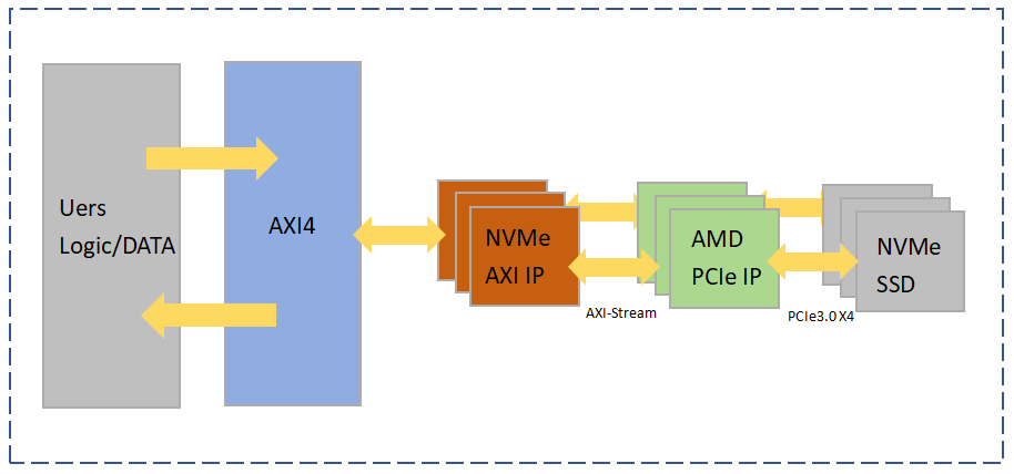
NVMe AXI FPGA IP Core interacts through the AXI4 bus protocol standard interface and implements PCIe Bridge internally, supporting both AXI Master FULL and AXI Stream versions. Interact with AMD PCIe IP through RC/RQ/CC/CQ AXI Stream interface to achieve read and write to external memory NVMe M.2 SSD without relying on CPU, compatible with NVM Express 1.4 protocol, and supports PCIe Gen 1.0, 2.0, 3.0, 4.0.
NVMe AXI FPGA IP Core provides you with fast and reliable, low-cost, high read/write bandwidth, and scalable performance solution, significantly reducing time to market.
NVMe AXI FPGA IP Core supports AMD/Xilinx Zynq UltraScale+ RFSoC, Zynq UltraScale+ MPSoC, Virtex UltraScale+, Kintex UltraScale+, Artix UltraScale+, Virtex UltraScale, Kintex UltraScale, Virtex 7 series of FPGA devices that meet the requirements of embedded systems for using SSDs, suitable for high bandwidth read and write, high-speed data storage, and high expansion scenarios.
Applications
● Data Center
● Cloud Computing Storage
● Enterprise Storage
● Intelligent Security
● AI
● Machine Learning
● Edge Computing
● Data Collection and Simulation of Autonomous Vehicles
● Medical/Industrial Testing Equipment
● Aerospace data acquisition and storage
● Analog digital signal data acquisition and storage
● Ethernet TCP/UDP network packet capture
Key Features
● Not relying on CPU, but reading and writing NVMe M.2 SSD through AMD FPGA device integrated PCIe IP core
● Support Commands: Identify, Write, Read, and Flush.
● Compatibility with NVM Express 1.4 protocol.
● Support PCIe Gen 1.0,2.0,3.0,4.0.
● Auto-initializes NVMe and PCIe link hardware modules.
● Automated submission and completion of commands.
● Supports a maximum of 65535 I/O commands per queue.
● Based on PCIe 3.0 X4, read/write rates up to 3000MB/s.
● MPSMIN (Minimum page size): 4K bytes.
● MDTS (Max data transfer size): 128K bytes or unlimited.
● LBA unit: 512 bytes or 4096 bytes.
● NVMe AXI FPGA IP Core supports the AXI Master FULL version and the AXI Stream version two versions.
● Reference Design Implementation: XCZU19EG + FMC Card (FH1402) + SAMSUNG 980 M.2 SSD
● Full technical support and custom design services

| Item ID | 102753 |
| Condition | New |
| Legacy item ID | |
| Model | NVMe AXI Stream/FULL |
| Manufacturer | Alinx Electronic Limited |
| Manufacturing country | China |
| Content | 1 piece |
| Weight | 1000 g |
| Customs tariff number |
NVMe AXI FPGA IP Core Application Interaction

The NVMe AXI IP interacts via the AXI4 standard interface and includes an internal PCIe Bridge, interfacing with AMD UltraScale+ Devices Integrated Block for PCI Express IP through the RC/RQ/CC/CQ AXI Stream interface. Achieved read/write operations on external NVMe SSDs without CPU involvement.
For more details on UltraScale+ Devices Integrated Block for PCIExpress IP, refer to the “PG213” document.
Illustrative Examples
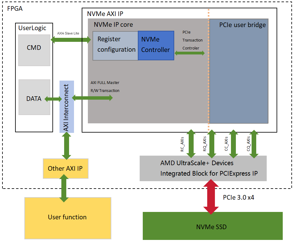
NVMe AXI Master FULL IP Vision

AXI Read/Write:
When the clock signal is active and the reset signal is low, the NVMe AXI IP begins automatic initialization. After initialization and link establishment, the user data stream is written through the AXI Interconnect IP to the AXI Master FULL interface of the NVMe AXI IP for interaction with queue management doorbell logic interaction in the NVMe protocol. The data forms TLP-layer PCIe packets, connecting to the UltraScale+ Devices Integrated Block for PCI Express IP from AMD via the RC/RQ/CC/CQ AXI Stream interfaces, and is sent to the NVMe SSD for storage. The NVMe AXI IP reads data from the NVMe SSD through the RC/RQ/CC/CQ AXI Stream interface and outputs it via the AXI Master FULL interface through the AXI Interconnect IP, allowing it to be accessed by any IP on a standard AXI bus for user logic implementation.
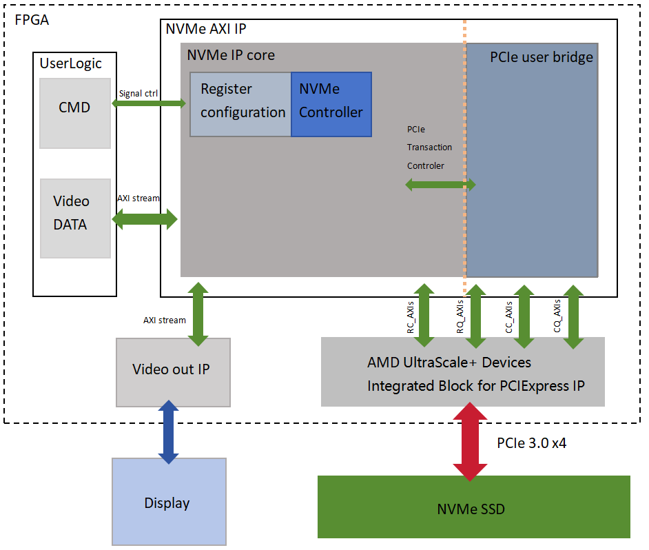
NVMe AXI Stream IP Vision

AXI Stream Read/Write:
When the clock signal is active and the reset signal is low, the NVMe AXI IP begins automatic initialization, After initialization and link establishment, the user’s data stream is written into the NVMe AXI IP through the AXI Stream interface for interaction with queue management doorbell logic interaction in the NVMe protocol, then forms TLP-layer PCIe packets, connecting via the RC/RQ/CC/CQ AXI Stream interface to AMD’s UltraScale+ Devices Integrated Block for PCI Express IP, and outputs data to the NVMe SSD for storage. The NVMe AXI IP reads data from the NVMe SSD via the RC/RQ/CC/CQ AXI Stream interface and outputs it through the AXI Stream interface to the video out IP for display.
IP Resource Utilization Table
The evaluation of IP resource consumption adopts AMD Zynq Ultrascale+ MPSoC series FPGA Development Kits/boards, which provides a fully functional design platform for building data storage acceleration applications. The AMD Zynq Ultrascale+ MPSoC series FPGA development boards/Kits provides an out of the box hardware platform with reference designs, which can shorten development time and allow you to focus on your target applications.
| Chip Model | Device Series | Frequency (MHz) | CLB Regs | CLB LUTs | CLB | BRAM Tile |
|---|---|---|---|---|---|---|
| XCZU19EG-FFVC1760-2-I | Zynq Ultrascale+ MPSoC | 250 | 8286 | 8459 | 1741 | 5 |
Note: Actual IP resource consumption is affected by the consumption of other logical resources during instantiation.
What do we offer?
Please contact us for more details.
Product Matrix
IP Information
Documentation
NVMe AXI Stream/Master FULL IP Core User Guide
IP Provided Format
Encrypted Netlist
Design Language
Verilog
Development Tool
Vivado 2020.1
Supported Devices
AMD/Xilinx Zynq UltraScale+ RFSoC, Zynq UltraScale+ MPSoC, Virtex UltraScale+, Kintex UltraScale+, Artix UltraScale+, Virtex UltraScale, Kintex UltraScale, Virtex 7
